Function Generator
This is an 80MHz function generator inspired by the Agilent 33250A. It supports waveforms up to 64k samples with 14-bit output resolution. The output level is only 1Vpp.
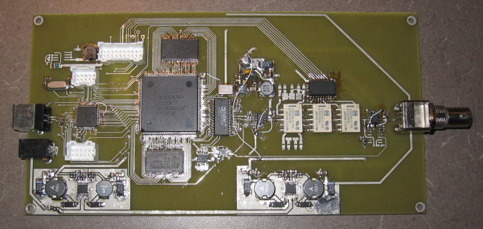
Design
The DAC is an AD9744 running at 200MHz. The FPGA (a Xilinx XC3S500E) multiplies the 50MHz clock to 100MHz for the DDS logic and 200MHz for the DAC. There are two RAMs (CY7C1021DV33-10) which are accessed at 100MHz. The DDS logic is duplicated so two consecutive output samples can be read simultaneously, keeping the clock speed of all the logic at 100MHz. The two output samples are interleaved and sent to the DAC at 200MHz.
The large FPGA is overkill but it allows for possible fancy features like IFFT signal generation. It also has lots of fast internal memory that could be used for modulation.
Using two seperate RAMs allows for either 64k samples at 200MHz or 128k samples at 100MHz. I haven't implemented the slow mode yet because I haven't needed such long waveforms.
Lessons Learned
- The LPC2141 has some open-collector pins which are not suitable for use on a data bus. Don't use GPIO on an LPC2xxx as an external bus.
- The original bus design had weird control signals that were a lot of trouble to implement. Stick to the usual /RD and /WR.
- The footprint for the chip driving the relays was too narrow. Always check the width of SOIC footprints.
- The Cuk converter makes a lot of noise. I've never had a switcher make such a whine. Choosing the right inductors is important to reduce this, but it is still audible and it clicks on power-up.
- The connectors all hang off the board in different amounts. They should have been aligned.
- I'm using asynchronous 10ns static RAM like pipelined synchronous RAM. It works, but I think I'm running too close to the timing specifications. I would have a lot more confidence in this design if the RAM were faster or synchronous.
- The four switching power supplies are overkill.